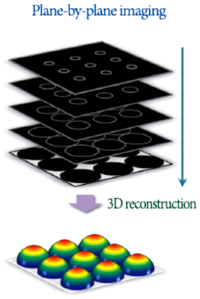
Image scanning is fast, and vertical scanning and measurement can be performed directly. It is suitable for the surface and inner layer analysis of wafers, semiconductors, LED materials, and can also be used for protein fluorescence and gene fluorescence image analysis.
System Introduction:
★ 3-D Dynamic Analyses
★ 3-D Imaging Construction
★ Depth Scanning and Measurement


feature of product
- - Suitable for all commercially available microscopes
- - Resolution: 512 × 512 pixel
- Image update rate: 5 frame / sec (512 × 512 pixel) - - Optional conjugate focus automatic control slit
- 400nm – 750nm detection range, optional other wavelength detection range
- Can be equipped with up to 2 PMT detectors
feature of product
★ Material surface and inner layer, wafer, semiconductor and LED analysis
★ Analysis of Fluorescent Protein and Gene Fluorescence Image
★ Multiple fluorescent images
★ 3D Carcass image reconstruction
specification:
Laser | 405nm, 470nm, 488nm, 532, nm 561nm, 635nm, 658nm, Selectable source Power control : continuous step ( related driver module) |
Microscope | Compatible to every microscope body. (needed to video port) To combine with every type of commercial microscope: Leica microscope, Zeiss microscope, Nikon microscope, Olympus microscope, Upright and Inverted and etc. |
Scanner type | Two galvanometer optical scanners |
Scan resolution | 128*128 pixel , 256*256 pixel, 512*512 pixel |
Scan speed | 1.5 frame per second ( 512*512 pixel) |
Scan zoom | 1X-16X ( optical zoom) |
Confocal Pinhole | Fixed pinhole, or 16-position motorized pinhole |
Detection range | 400nm-750nm or customizable [PMT] |
Number of detector | Up to 2 , or customizable |
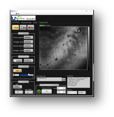
Software | Language : LabView Main function: Operation/ Image processing/ Color merge Line profile/ Histogram |


