MultiView 4000
Multi-Probe Optically Integrated AFM-Raman-NSOM
MultiView 4000
Multi-Probe Optically Integrated AFM-Raman-NSOM
Israel's NANONICS is the industry's leading brand that combines near-field optical microscope (NSOM) technology and atomic force microscope (AFM) technology, and is one of the most experienced companies in this category of products. Coupled with its strong system integration capabilities, all material characterization analysis is integrated on one experimental platform, and the following types of imaging analysis experiments can be performed immediately or simultaneously including:
★ Multi-Probe SPM Functions
★ NSOM
★ AFM
★ Confocal Imaging
★ Thermal couple Imaging
★ Thermal Resonance Imaging
★ Electrical Conductance
★ Kelvin Probe Microscopy
★ Piezo Force Microscopy
★ Magnetic Force Microscopy (Variation of Magnet)
★ Electrical Force Microscopy
★ Scanning Electr0-Chemical Microscope (SECM)
★ Tip Enhanced Raman Scattering (TERS)
★ SEM-AFM Combination
★ AFM-IR-THz-Raman


Near-field optical experiment ↓


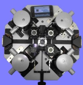
Up to 4 AFMs in One System
- • Four probes operate simultaneously and independently, with each probe having its own feedback and scanning capabilities.
- • Measure sophisticated properties only possible with the availability of multiple probes such as electrical, thermal and optical properties of devices
- • The MultiView 4000is a novel platform containing multiple probes/AFM's for advanced experiments such as: nanoscale transport, optical pump-probe, read-write experiments.
The MV 4000 continues the tradition of the MV series of providing total optical flexibility and customization possibilities so that now AFM Raman and tip enhanced Raman spectroscopy (TERS) can be integrated with the multiprobe capability. Finally, free optical access from above allows easy visualization of all probes and facilitates nanomanipulation.
The MV 4000 product brochure can be downloaded here.
The simultaneous and independent SPM probe operation of up to 4 probes enables full characterization of all dimensions of samples and devices. All forms of SPM are enabled for each individual probe accompanied by total optical integration resulting in access to all modes including AFM, KPM, EFM, ANSOM, NSOM, STM, AFM-Raman, and TERS. Because these probes are designed for multiple probe operation, they can be brought to a nanometric separation distance thus ensuring that the same area is scanned with all the probes.
Multiprobe capability is especially useful for electrical measurements since multiple probes can now be placed over the element to provide bias or probe its conductivity, resistance, etc just like in a probe station. Two-, three-, or four-point resistance measurements are possible. Multiple probes also enable flexible positioning and manipulation to provide bias, localized I-V measurements, and multichannel imaging.
One probe can be the source of excitation while the second probe follows the transport process with high spatial resolution. Alternatively, optical pump/probe experiments can now be performed using one probe to optically pump while the other probe measures the optical output in a variety of configurations. An example of each type of measurement is shown below.
Thermal transport measurement within an SRAM device where heat is introduced at specific locations and detected at other locations. As contact is made in different regions of the SRAM with the thermal conductivity probe, the probe tip cools to different levels depending on the material's thermal conductivity. The resulting image is obtained by determining the current alterations that had to to be affected in order to keep the current flowing past the point resistance at a constant value.
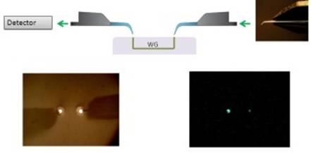
With two cantilever, near-field optical probes with exposed tips, light is injected through one probe and is guided through the sample which is a fiber. With the second probe in place, this injected light can be collected and analyzed both spatially and temporally. In this image two NSOM probes are seen in AFM contact with the input and output of the fiber waveguide.
See a video showing an example using multiprobe technology to conduct nanothermal measurements here.
With a multiprobe system, resolution and tip quality no longer need to be compromised since each probe is now individualized for each measurement. In classic NSOM setups the NSOM probe would have the dual function of imaging topography and fluorescence where the topography image is compromised by the aperture (wider diameter) needed by the NSOM probe. But in a multiprobe setup, a standard SPM probe can be used the topography without affecting the NSOM fluorescence measurement.

The left and center images are the topography and fluorescence images, respectively, of lumogen dye particles collected in a multiprobe setup with different probes for topography and NSOM. The image on the right is the topography image of the same sample but collected with the NSOM probe, revealing the clear loss of resolution and morphology. The width of each image is 8um.
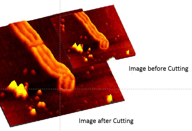
One probe can be used for moving, cutting, or positioning a sample, while the other probe can be used to image the sample. For example, shown below is a chromosome that has been dissected with one probe (see image on left), while the other probes images the result of the nanomanipulation.
|
|
|
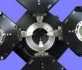
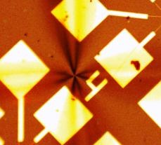
(Left) MultiView 4000TM four SPM probes platform. (Middle) MultiView 4000TM Tip and | ||
The images above show the procedure that can be implemented to bring two or more probes in close proximity to one another. Specifically in the images shown the common features in a carbon nanotube sample are imaged by two probes and from these images it is clear that the two probes are displaced along the y axis by 300nm and along the x axis by 1.7microns |


